


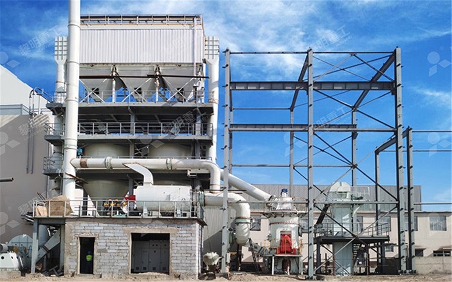
HOME→Silicon dioxide processing technology Silicon dioxide processing technology Silicon dioxide processing technology
MTW European Type Trapezium Mill
Input size:30-50mm
Capacity: 3-50t/h

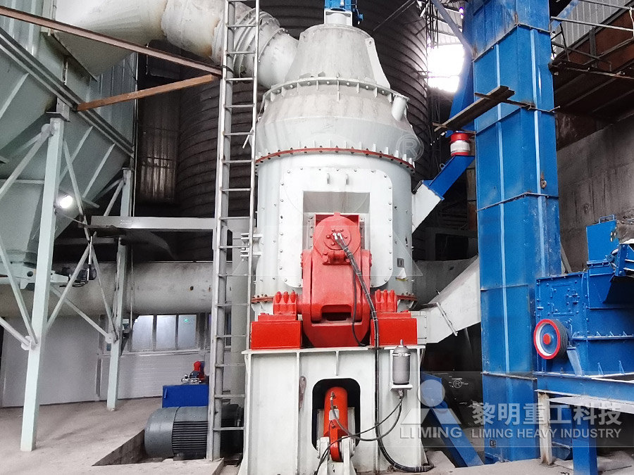
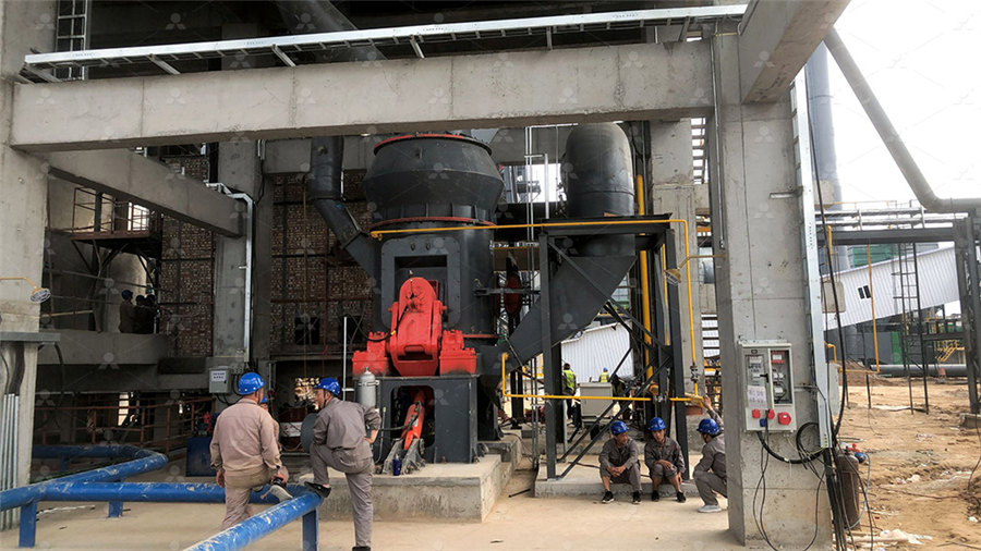
LM Vertical Roller Mill
Input size:38-65mm
Capacity: 13-70t/h
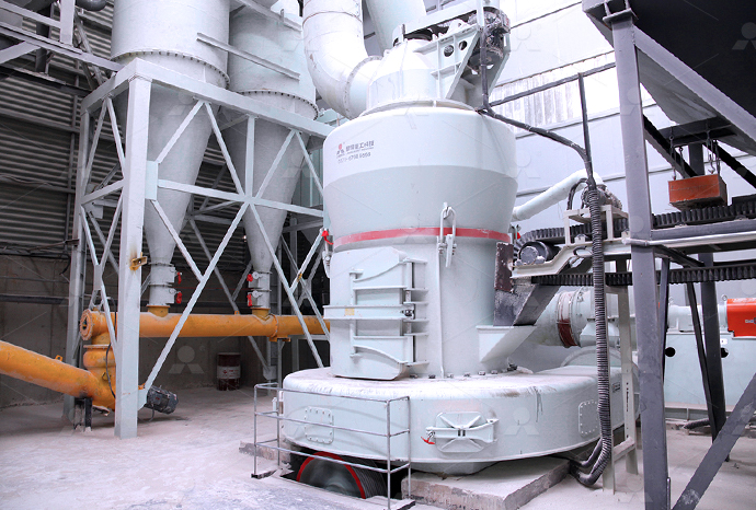
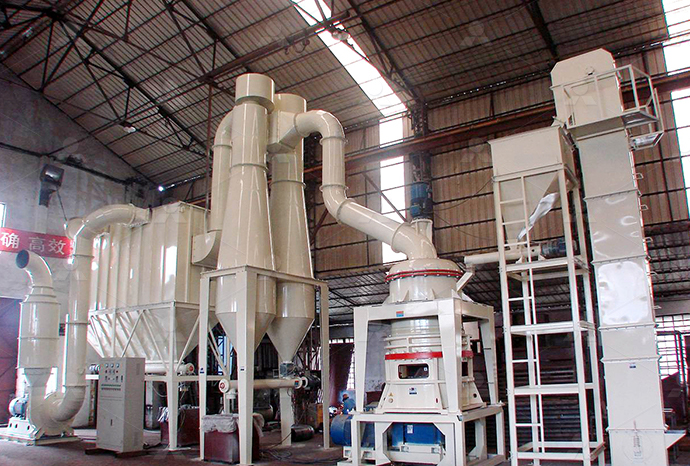
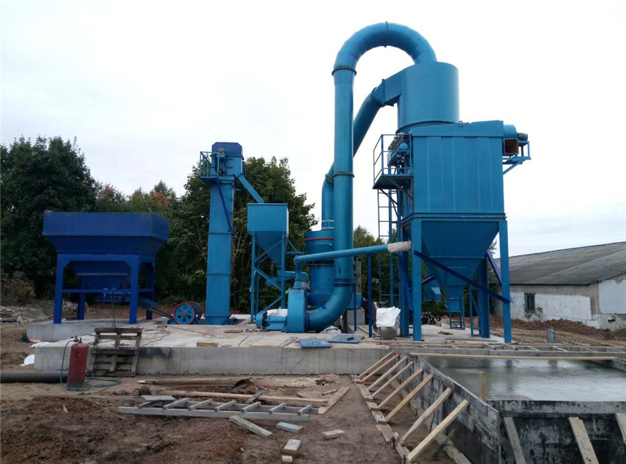
Raymond Mill
Input size:20-30mm
Capacity: 0.8-9.5t/h
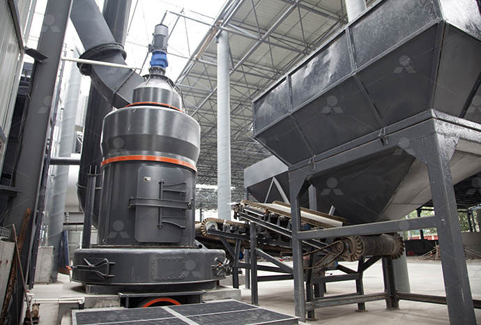
Sand powder vertical mill
Input size:30-55mm
Capacity: 30-900t/h
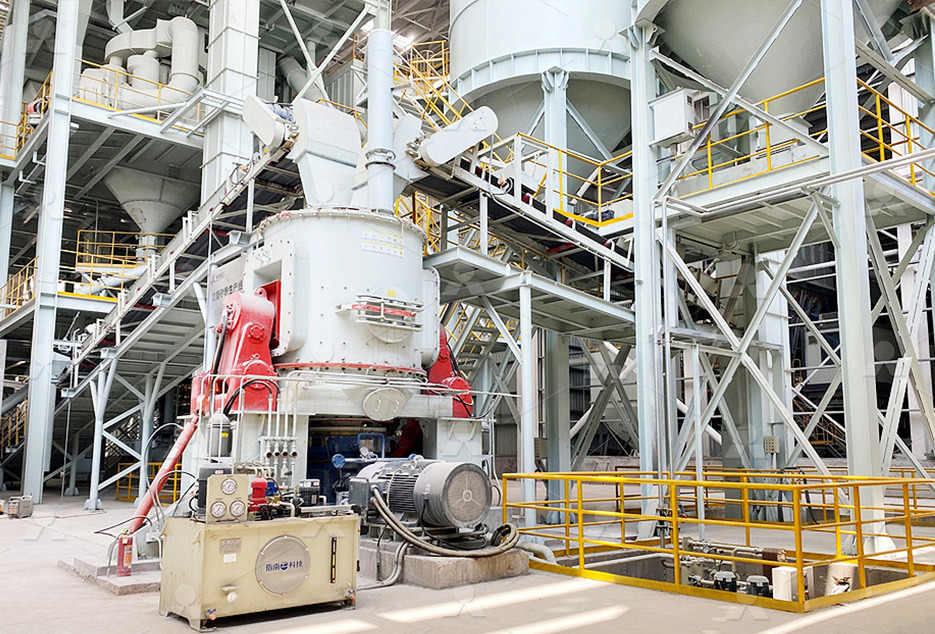
LUM series superfine vertical roller grinding mill
Input size:10-20mm
Capacity: 5-18t/h
MW Micro Powder Mill
Input size:≤20mm
Capacity: 0.5-12t/h
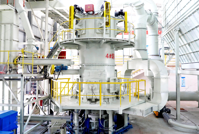
LM Vertical Slag Mill
Input size:38-65mm
Capacity: 7-100t/h
LM Vertical Coal Mill
Input size:≤50mm
Capacity: 5-100t/h
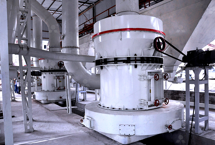
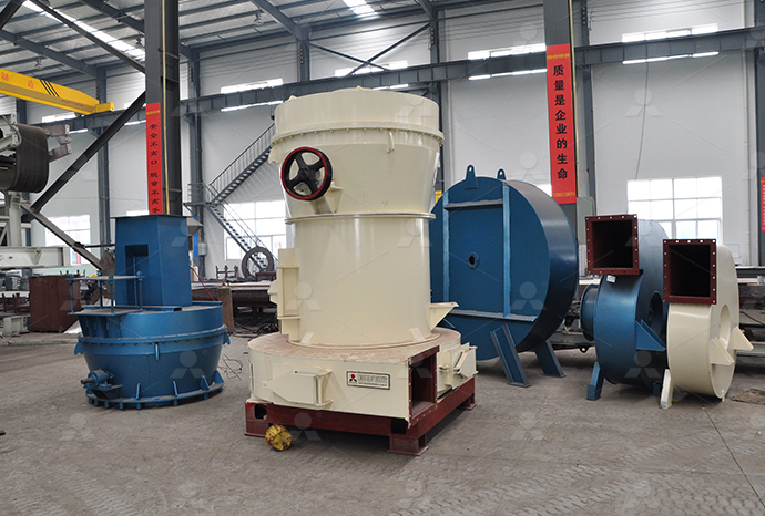
TGM Trapezium Mill
Input size:25-40mm
Capacity: 3-36t/h
MB5X Pendulum Roller Grinding Mill
Input size:25-55mm
Capacity: 4-100t/h
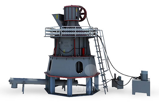
Straight-Through Centrifugal Mill
Input size:30-40mm
Capacity: 15-45t/h
Silicon dioxide processing technology Silicon dioxide processing technology Silicon dioxide processing technology
.jpg)
Silicon Dioxide an overview ScienceDirect Topics
Silicon dioxide is a commonly used insulator material in IC technology and silicon device fabrication It refers to the process of chemically growing silicon dioxide on the surface of a Silicon dioxide is the most commonly used insulator material in IC technology and in the other fields of silicon device fabrication technology This chapter explains the various aspects of the Silicon Dioxide an overview ScienceDirect Topics2003年5月18日 Silicon dioxide (SiO 2) is conventionally reduced to silicon by carbothermal reduction, in which the oxygen is removed by a heterogeneous–homogeneous reaction Pinpoint and bulk electrochemical reduction of insulating silicon 2019年12月18日 Here, we demonstrate a simple process for making highpurity solargrade silicon films directly from silicon dioxide via a onestep electrodeposition process in molten salt Electrodeposition of crystalline silicon films from silicon dioxide for
.jpg)
SiO 2 thin film growth through a pure atomic layer deposition
Silicon dioxide (SiO 2) and more generally ultrathin oxide films have been extensively described as good components for modern nanotechnologies such as dielectric materials in silicon 1989年3月1日 Polycrystalline silicon–silicon dioxide–silicon capacitors were annealed in argon and argon containing oxygen ambients in a rapid thermal annealer Capacitance–voltage Rapid thermal processing of silicon dioxide films in metal–oxide 2018年2月22日 Here we demonstrate in a combined crossed molecular beam and computational study that silicon dioxide (SiO 2) along with silicon monoxide (SiO) can be Directed gas phase formation of silicon dioxide and Nature1990年11月1日 The 20 to 100‐nm thick tetraethylorthosilicate (TEOS)‐derived SiO 2 films were deposited on silicon substrates in the 650–780 °C temperature range by low‐pressure Properties of silicon dioxide films prepared by low‐pressure
.jpg)
21 Silicon Dioxide Properties TU Wien
21 Silicon Dioxide Properties The growth of silicon dioxide is one of the most important processes in the fabrication of MOS transistors The attributes of SiO which make it appealing Silicon Dioxides Simo Eränen, in Handbook of Silicon Based MEMS Materials and Technologies, 2010 Publisher Summary Silicon dioxide is the most commonly used insulator material in IC technology and in the other fields of silicon device fabrication technology This chapter explains the various aspects of the growth and deposition of silicon dioxidesSilicon Dioxide an overview ScienceDirect Topics2000年4月1日 Request PDF Low Temperature Silicon Nitride and Silicon Dioxide Film Processing by Inductively Coupled Plasma Chemical Vapor Deposition High‐density plasma technology is becoming Low Temperature Silicon Nitride and Silicon Dioxide Film Processing 2020年8月7日 Vasiliyev has also published a series of review articles that more broadly examines silicon nitride technology 9–14 While oxygen incorporation into silicon nitride is part of this review, films where the objective is formation of pure silicon oxynitride are not included and are the subject of a separate review 15Review—Silicon Nitride and Silicon NitrideRich Thin Film
.jpg)
Silicon Dioxide Structure, Properties, Uses of SiO2
Silicon Dioxide is a chemical compound with the formula SiO2 Visit BYJU'S to understand the properties, structure and uses of Silicon Dioxide (SiO2) explained by India's best teachers2000年5月1日 Journal of Vacuum Science Technology B: Microelectronics and Nanometer Structures Processing, Measurement, Article Navigation Research Article May 01 2000 Hydrogen diffusion through silicon/silicon dioxide interfaces N H Nickel N H Nickel HahnMeitnerInstitut Berlin, Kekuléstr 5, D12489 Berlin, GermanyHydrogen diffusion through silicon/silicon dioxide interfacestechnology since it requires only supercritical CO2 and a small amount Thickness measurementswere taken before and after processing; silicon and silicon dioxide etch rates as low as 2 Å/min SUPERCRITICAL CARBON DIOXIDE: THE NEXT GENERATION 2016年7月31日 From a nanofabrication standpoint, once a single crystal cylindrical ingot of silicon is grown and cut into circular wafers (roughly 12 inches in diameter and 05 mm thick at present and most often covered with a submicron layer of silicon dioxide or other dielectrics), the principal patterning step (2) that generates nanoscale features in the lateral dimension is Silicon Planar Processing and Photolithography SpringerLink
.jpg)
(PDF) SiO2 surface passivation layers – a key technology for silicon
2018年6月22日 From passivating coatings and masking layers for diffusion to ultrathin tunneling films — all the silicon technology could not exist without silicon dioxide2007年12月1日 For excellent accounts of the early Fairchild work and its wider implications, see Gordon Moore’s “The Role of Fairchild in Silicon Technology in the Early Days of ’Silicon Valley’ ” and The Silicon Dioxide Solution IEEE Spectrum2023年11月20日 In nonporous form, silica nanoparticles are used as abrasives and absorbents Therefore, meso and macroporous silicas with ordered structures have great potential in several applications, such as catalysis, adsorption, nanomedicine, biotechnology and pharmaceutical technology (drug delivery), and electrochemistry (sensors and supercapacitors)Synthesis and Application of Silicon Dioxide Nanoparticles1996年9月1日 The chemical dry etching of silicon nitride (Si 3 N 4)and silicon nitride (SiO 2) in a downstream plasma reactor using CF 4, O 2, and N 2 has been investigated A comparison of the Si 3 N 4 and SiO 2 etch rates with that of polycrystalline silicon shows that the etch rates of Si 3 N 4 and SiO 2 are not limited by the amount of fluorine arriving on the surface onlyChemical dry etching of silicon nitride and silicon dioxide using CF
Strain Measurements of Silicon Dioxide Microspecimens by
2007年2月3日 Silicon dioxide (SiO 2) is an integral part of the integrated circuit and microelectromechanical systems (MEMS) architectureThe ability to thermally grow high quality oxide films coupled with the insulating properties of SiO 2 has spurred the technological advances of the semiconductor industry based on Si processing [1–3]Important uses for SiO 2 include Silicon is the second most abundant element in the earth’s crust, second only to oxygen It is naturally found as fairly pure silicon dioxide and as silicates The silicon dioxide is found as huge deposits of quartzite or quartz sand Moreover, many rocks contain quartz crystals Therefore, it can be concluded that theSilicon processing: from quartz to crystalline silicon solar cellsMicro Mechanical Systems Michael L Reed, Gary K Fedder, in Handbook of Sensors and Actuators, 1998 223 SiO 2 Silicon dioxide, SiO 2, is an amorphous material used in microsystems as a dielectric in capacitors and transistors; as an insulator to isolate various electronic elements; and as a structural or sacrificial layer in many micromachining processesSilicon Dioxide (Sio2) an overview ScienceDirect Topics2024年7月11日 Explore the world of Silicon Dioxide (SiO₂) 🌐: From its crystalclear role in glass to shaping tech foods Dive into its secrets benefits! Subjects English; Maths; Chemistry; Its versatile nature allows it to be used in a wide range of industries, from construction and manufacturing to food processing and technology, Silicon Dioxide ( SiO₂) Definition, Structure, Preparation, Uses
Etching of glass, silicon, and silicon dioxide using negative ionic
2018年9月7日 Ionic liquid ion sources have been proposed as a new type of ion source for focused ion beam and broad ion beam applications In this paper, the ionic liquid EMIBF 4 (1ethyl3methylimidazolium tetrafluoroborate) was used as an ion source to generate negatively charged ions and irradiate glass (Pyrex 7740), silicon, and silicon dioxide targets2023年6月1日 Silicon is the most widely used semiconductor material in the field of integrated circuits (ICs) and photovoltaic industry due to its abundance, low cost, and remarkable synergy with silicon dioxide [1], [2], [3], [4]In the manufacture of ICs, chemical mechanical polishing (CMP) is employed as the only global planarization technology for processing silicon wafers [5, 6]High efficiency chemical mechanical polishing for silicon wafers Silicon and silicon dioxide are two important materials in the field of electronics and technology While they are both composed of silicon atoms, they have distinct properties and applications In this article, we will compare the attributes of silicon and silicon dioxide to understand their differences and similaritiesSilicon vs Silicon Dioxide What's the Difference? This vs That2017年2月27日 Etch rate enhancement of 7–8 for silicon and 3–4 for silicon dioxide have been obtained over pure physical etching A chemical flux of sulfur “Electron cyclotron resonance microwave discharges for etching and thin film deposition,” inHandbook of Plasma Processing Technology, Noyes Publications, New Jersey (1990), Chemically assisted ion beam etching of silicon and silicon dioxide
Silicon on Insulator (SOI) Technology PPT Free
2017年12月9日 19 BESOI (Bond and Etchback SOI) SOI Technologies By using bonding chemistry between silicon (Si) and silicon dioxide(SiO2) or between SiO2 and SiO2 effectively, two Si wafers are tightly bonded with a 1990年11月1日 Properties of silicon dioxide films deposited at low temperatures by microwave plasma enhanced decomposition of tetraethylorthosilicate J Vac Sci Technol B (May 1992) Synthesis and characterization of SiO 2 films deposited using tetraethylorthosilicate/ozone at low processing pressures (10 −1 to 10 −3 )Properties of silicon dioxide films prepared by low‐pressure Summary Many processing steps are required to fabricate complex electronic devices, including doping by ion implantation, patterning, etching, passivation, and metallization The process flow in SiC device fabrication is similar to that in silicon technology but several unique processes, with particular requirements, Device Processing of Silicon Carbide Wiley Online Library2023年8月3日 In semiconductor technology, silicon dioxide (SiO 2) films are required as insulating layers for the electrical function of the componentsHigh quality oxide layers grow in dry or wet oxygen atmosphere at high temperature using silicon from the substrate, leading to segregation effects and interface chargesOxidation of Silicon SpringerLink
Remote plasma etching of silicon nitride and silicon dioxide using
1998年7月1日 The etching of silicon nitride (Si 3 N 4) and silicon dioxide (SiO 2) in the afterglow of NF 3 and NF 3 / O 2 microwave discharges has been characterized The etch rates of both materials increase approximately linearly with the flow of NF 3 due to the increased availability of F atoms The etch rate of Si 3 N 4 is enhanced significantly upon O 2 injection into the NF 3 1999年11月1日 AVS: Science and Technology of Materials, Interfaces and Processing ; Chinese Physical Society ; Hefei General Machinery Research Institute ; Laser Institute of America ; (Si 3 N 4) layers from silicon and silicon dioxide (SiO 2) is described and its mechanism examinedHighly selective etching of silicon nitride over silicon and silicon 2013年8月1日 The coating of titanium dioxide nanoparticles with silicon dioxide has been carried out by dielectric barrier discharge (DBD) plasma treatments to enhance the thermostability of Titania for applications at high temperature processes During the first coating processing step, a closed film of silicon nitride was produced via plasma treatment in a gaseous mixture of silane Silicon Dioxide Coating of Titanium Dioxide Nanoparticles from 200 300 400 500 600 700 800 0 200 400 600 800 1000 A r 7635 A r 7503 A r 8115 H 2 6562 H 2 4861 S iH 4142 N 2 3371 13SiH4 /9 N2 /20A r 800 W ICP 120 W rf Intensity (ab unit) 10 m TorrDEVELOPMENT OF LOW TEMPERATURE SILICON NITRIDE AND SILICON DIOXIDE
Pyrometallurgy Towards Clean Metallurgical Processing 2012
letic silicon dioxide is easy to organize in industlial "URGICAL PROCESSING 239 ms into a gaseous state Gaseous (NH4)2SiF6 is :ompanies with regeneration of the fluorinating agent OH = + 6NH4F + 2H20 (3) filtration from the solution of ammonium fluoride vaporated and cwstallized in the form of technical 75% NH4F HE Silicon dioxide in finely Magic silicon dioxide for widely tunable integrated photonics Bruno LopezRodriguez1* †, Naresh Sharma 1, Zizheng Li , Roald van der Kolk 1, Jasper van der Boom , Thomas Scholte , Jin Chang 2, Simon Gr¨oblacher , Iman Esmaeil Zadeh1 1Department of Imaging Physics (ImPhys), Faculty of Applied Sciences, Delft University of Technology, Lorentzweg 1, Delft, 2628 CJ, TheMagic silicon dioxide for widely tunable integrated photonicsSilicon Nitride, Silicon Dioxide, and Emerging Dielectrics 10 (Table of Contents) Author: Electrochemical Society \(ECS\) Subject: ECS Transactions Volume 19 No02 Keywords: SILICON NITRIDE, SILICON DIOXIDE, AND EMERGING DIELECTRICS 10 (215TH ECS MEETING) Created Date: 4/24/2017 9:09:35 AMSilicon Nitride, Silicon Dioxide, and Emerging Dielectrics 年10月1日 This article provides an overview of the stateoftheart chemistry and processing technologies for silicon nitride and silicon nitride rich films, ie, silicon nitride with C inclusion, both in (PDF) Silicon Nitride and Silicon NitrideRich Thin Film
Processing and kinetics studies on the alumina enrichment of coal
2010年2月1日 Fuel Processing Technology Volume 91, Issue 2, February 2010, Pages 175184 Processing and kinetics studies on the alumina enrichment of coal fly ash by fractionating silicon dioxide as nano particles Author links open overlay panel Guanghui Bai a, Wei Teng a, Xianggang Wang a, Hui Zhang b, Peng Xu a Show more Add to Mendeley 4 NonMetallic Material Science V 02 01 2020 40 0 5 10 15 20 497 517 537 557 577 597 617 Figure 6 Generalized radius versus time 5 Deviation Model based on Melting RateSolving the Problem of Silicon Dioxide Melting Based on2023年11月28日 This chapter reviews the Si waferprocessing technology, including ingot heat treatment, cutting, slicing, lapping, polishing, LP Hunt, Handbook of Semiconductor Silicon Technology (Noyes Publications, 1990) Google Scholar G Müller, Review: The Czochralski method – Where we are 90 years after Jan Czochralski’s invention Silicon Wafer Processing SpringerLinkSilicon Nitride and Silicon Dioxide Thin Insulating Films: Proceedings of the Sixth International Symposium Volumes 20012007 of Proceedings (Electrochemical Society) Author: Electrochemical Society Dielectric Science and Technology Division: Editor: K B Sundaram: Contributors: Electrochemical Society Electronics Division, Electrochemical Silicon Nitride and Silicon Dioxide Thin Insulating Films
Modeling the plasma chemistry of C2F6 and CHF3 etching of silicon
2001年9月1日 A detailed chemical reaction mechanism is reported that describes the C 2 F 6 and CHF 3 plasma etching of silicon dioxide, which is widely used in the fabrication of microelectronic devices The gasphase part of the C 2 F 6 mechanism involves 28 species and 132 reactions, while the surface part involves 2 materials, 6 species, and 85 reactions Rate In thermal oxidation with silicon, the silicon reacts with oxygen to form silicon dioxide The ratio of the grown oxide layer and of used up silicon is 227, which means that the dioxide is growing into the silicon substrate by 45 % of the total thickness of Fabrication of oxide layers Oxidation Semiconductor Technology 1989年3月1日 Joseph Z Xie, Harvey Kauget, Shyam P Murarka; Rapid thermal processing of silicon dioxide films in metal–oxide semiconductor capacitors: High‐temperature SiO 2 decomposition at the SiO 2 –Si interfaces in inert ambient Journal of Vacuum Science Technology B: Microelectronics Processing and Phenomena 1 March 1989; 7 (2): 141–144Rapid thermal processing of silicon dioxide films in metal–oxide 2024年9月7日 Steps and Technology involved Silicon wafer is the foundation of all modern semiconductor manufacturing It is the base, heart and backbone of all semiconductors and modern electronics In this comprehensive guide, we’ll learn and understand the Silicon Wafer Manufacturing Process: Sand to Silicon – Steps and Technology involvedSilicon Wafer Manufacturing Process: Sand to Silicon